HDLBits刷题日记(二)
打算利用碎片化时间重温一遍Verilog语法,好记性不如烂笔头,在此记录一下HDLBits刷题的过程,记录一些知识点,方便日后再次复习。
1、Verilog Language - Basics
Problem 4 : Notgate
Create a module that implements a NOT gate.
创建一个模块,实现一个非门。
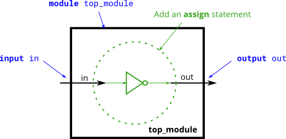
module top_module (
    input in,
    output out
);
    assign out = ~ in;

endmodule~是逐位取反。!是逻辑取反。
Problem 5 : Andgate
Create a module that implements an AND gate.
创建一个模块,实现一个与门。
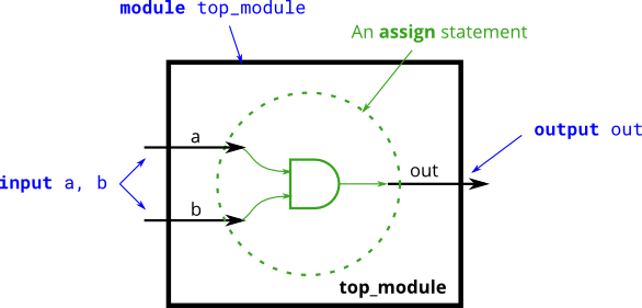
module top_module(
    input a,
    input b,
    output out
);
    assign out = a & b;

endmodule&是逐位与。&&是逻辑与。
Problem 6 : Norgate
Create a module that implements a NOR gate. A NOR gate is an OR gate with its output inverted. A NOR function needs two operators when written in Verilog.
创建一个模块,实现一个或非门。一个或非门是一个或门,其输出被反转。在Verilog中,一个或非函数需要两个运算符。

module top_module(
    input a,
    input b,
    output out
);
    assign out = ~(a | b);

endmodule|是逐位或。||是逻辑或。注意括号的由来,因为 ~ 非逻辑的优先级大于 | 或。
Problem 7 : Xnorgate
Create a module that implements an XNOR gate.
创建一个模块,实现一个同或门(异或非门)。
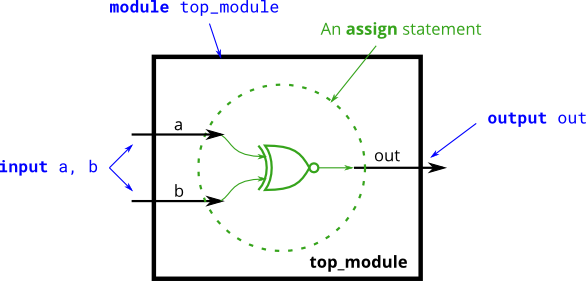
module top_module(
    input a,
    input b,
    output out
);
    assign out = ~(a ^ b);

endmodule
同或门 (XNor Gate) 是异或门 (Xor Gate) 的取反输出。
异或门的输入输出可以概括为:(输入)相同(输出)为 0 ,不同为 1。
^为逐位异或,Verilog 中不存在逻辑异或符号。
Problem 8 : Declaring wires
信号定义语句需要放置于模块的 body 中,模块的 body 指的就是 module 和 endmodule 中间的部分。
举个例子:
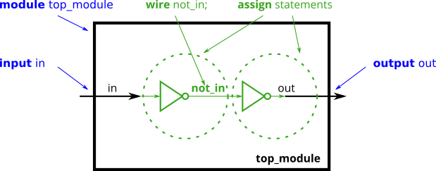
module top_module (
    input in,              // Declare an input wire named "in"
    output out             // Declare an output wire named "out"
);

    wire not_in;           // Declare a wire named "not_in"

    assign out = ~not_in;  // Assign a value to out (create a NOT gate).
    assign not_in = ~in;   // Assign a value to not_in (create another NOT gate).

endmodule   // End of module "top_module"
在上面的模块中,有三个 wire (in、out 和 not_in) ,其中两个已经声明为模块的输入和输出端口的一部分 (这就是为什么在前面的练习中不需要声明任何连接)。wire not_in 需要在模块内部声明。从模块外部不可见。然后,使用两个 assign 赋值语句创建两个 NOT 门。注意,先创建哪个 NOT 门并不重要,最终还是会得到相同的电路。
小试牛刀:
Implement the following circuit. Create two intermediate wires (named anything you want) to connect the AND and OR gates together.
实现以下电路:创建两个中间线 (命名任意) ,以便连接与门、或门一起。
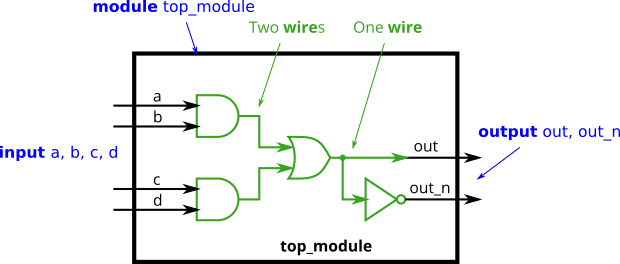
`default_nettype none

module top_module (
    input a,
    input b,
    input c,
    input d,
    output out,
    output out_n
);

    wire w1, w2;

    assign w1 = a & b;
    assign w2 = c & d;
    assign out = w1 | w2;
    assign out_n = ~out;

endmodule- 在定义信号的同时,可以对其赋值,如
wire w1 = a & b;。
Problem 9 : 7458
The 7458 is a chip with four AND gates and two OR gates.
7458 是一个具有四个与门和两个或门的芯片。
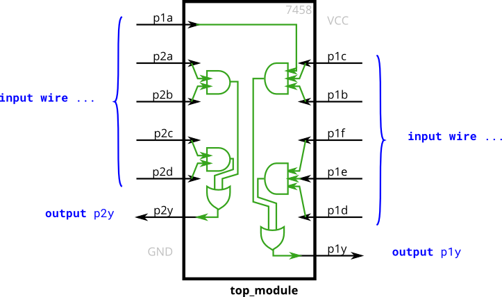
module top_module (
    input p1a,
    input p1b,
    input p1c,
    input p1d,
    input p1e,
    input p1f,
    output p1y,
    input p2a,
    input p2b,
    input p2c,
    input p2d,
    output p2y
);

    wire w1, w2, w3, w4, w5, w6;

    assign w1 = p1a & p1b & p1c;
    assign w2 = p1d & p1e & p1f;
    assign w3 = p2a & p2b;
    assign w4 = p2c & p2d;
    assign p1y = w1 | w2;
    assign p2y = w3 | w4;

endmodule
或者对每个输出信号,使用一个 assign 语句,不需要中间信号。
module top_module (
    input p1a,
    input p1b,
    input p1c,
    input p1d,
    input p1e,
    input p1f,
    output p1y,
    input p2a,
    input p2b,
    input p2c,
    input p2d,
    output p2y
);

    assign p1y = (p1a & p1b & p1c) | (p1d & p1e & p1f);
    assign p2y = (p2a & p2b) | (p2c & p2d);

endmodule
2、逻辑门总结
&是逐位与,而&&是逻辑与。~是逐位取反,而!是逻辑取反。|是逐位或, 而||是逻辑或。^为逐位异或,Verilog 中不存在逻辑异或符号。同或门 (XNor Gate) 是异或门 (Nor Gate) 的取反输出。
异或门的输入输出可以概括为:(输入)相同(输出)为 0 ,不同为 1。